
Intel 18A: From Risky Bet to Serious Contender
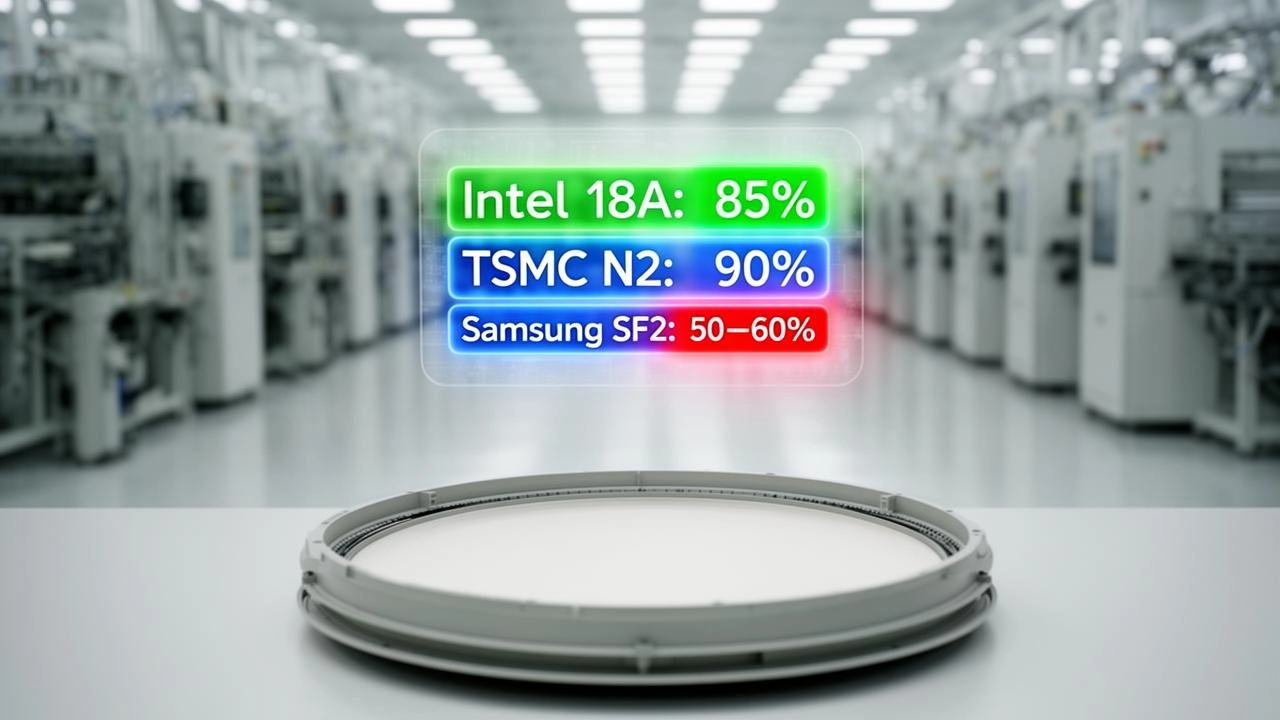
Intel’s 18A process is an advanced chip production technology aimed at delivering high transistor density and power-efficient performance, and its recent jump in semiconductor manufacturing yield from 65% to 85% signals a decisive move from early risk production towards a more mature, cost-efficient node for next-generation CPUs and GPUs. That single statistic is the big story: Intel has gone from being an underdog at cutting-edge nodes to sitting within striking distance of the leading foundry. According to a research report from KeyBanc Capital Markets, “the yield rate for Intel’s most advanced ‘Intel 18A’ process has significantly improved from a previous 65% to 85%.” For PC performance competition, that changes the narrative. The question is no longer whether Intel can manufacture at this level—it’s how fast it can scale and how aggressively it will price the silicon that enthusiasts care about.
Yield Numbers and Design Wins: Intel Joins the Top Tier
The 85% yield on the Intel 18A process narrows the gap with TSMC’s reported 90% yield on its N2 node while pulling far ahead of Samsung Foundry’s SF2 at 50% to 60%. In foundry terms, that is not a footnote—it is a turning point. Higher yields mean fewer dead dies per wafer, better economics, and the confidence big chip designers need before trusting a new process. That confidence is already visible: KeyBanc’s report notes that Intel has secured wafer foundry design orders for 18A and 14A from AMD, Nvidia, Marvell, Microsoft, Micron, OpenAI, and Apple’s low-end M‑series processors. For years, the advanced node story has been “TSMC or nothing.” Those design wins show that Intel 18A is now credible enough to sit beside N2 in vendor roadmaps, and that alone strengthens future CPU performance competition across desktops, workstations, and high-performance computing.
Self-Reliance on Nova Lake and the Packaging Offensive
Intel’s manufacturing progress is reshaping its own desktop strategy. KeyBanc reports that Intel previously intended to outsource about 60% to 70% of its upcoming Nova Lake desktop processor dies to TSMC because of performance tuning issues on 18A, but has now reversed course and plans to produce 80% to 90% of Nova Lake dies in-house on its own foundry lines. That is a bold bet on its Intel 18A process and on long-term control over CPU performance competition. At the same time, Intel’s advanced packaging push is quietly giving it another weapon. The yield for its EMIB‑T packaging tech has climbed from 90% to 98%, matching the reported 98% to 99% yield range of TSMC’s CoWoS. With high‑yield packaging already used in Nvidia’s Feynman GPUs, Google’s TPU HumuFish, and AWS Trainium 3 chips, Intel isn’t just catching up on the node; it is building an ecosystem that can host the most demanding CPUs and AI accelerators.
Ireland Fab Expansion: Capacity for Xeon Today, Headroom for Tomorrow
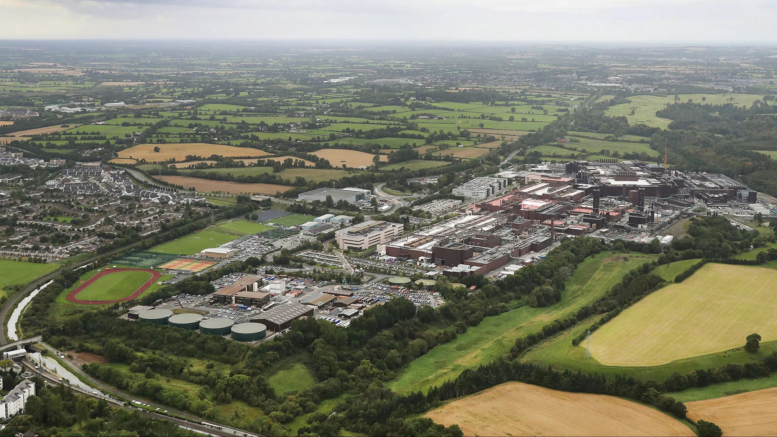
Raising yield is only half the battle; Intel also needs the fabs to push enough wafers through. That is where its Leixlip facility comes in. Intel has announced a €5 billion (USD 5.7 billion, approx. ₱332 billion) investment to expand and modernize manufacturing operations at its campus near Leixlip. The project targets increased output of Xeon 6 processors and next-generation Xeon products built on the Intel 3 process—a 3 nm‑class node—alongside advanced R&D work. Intel opened Fab 34 at this site in 2023 and it currently produces Core Ultra 100‑series on Intel 4 and Xeon 6 on Intel 3 using EUV tools. This fab is described as the only high‑volume semiconductor production facility in Europe using EUV lithography, and Intel has already bought back a 49% stake it sold in mid‑2024 for €10.1 billion to enable the current expansion. Kicking off execution earlier this year without a disclosed completion date, Intel is clearly preparing long-term capacity that can support both data center Xeon lines and spillover demand from cutting-edge consumer processors built on Intel 3 and, eventually, 18A.
Where This Leaves High-Performance PC Competition
Put together, Intel’s 18A yield gains, fresh design wins, and fab expansion mark a reset in advanced chip production. The company now reports 85% yield on its leading process, with 18A‑P in risk production and a 14A node tracking ahead on defect density, targeting mass production in the second half of 2028. It is also ramping capacity for 18A and Intel 3, with wafer equipment orders reportedly increased by 30% to 40%. On the packaging front, EMIB‑T’s 98% yield stands shoulder‑to‑shoulder with established CoWoS solutions. Meanwhile, Intel is investing billions into Leixlip to push more Xeon 6 and Intel 3 products through Europe’s only high‑volume EUV fab. For enthusiasts and high‑performance computing builders, the takeaway is clear: the next wave of CPU performance competition will not be a one‑foundry race. Intel is making the kind of manufacturing and packaging progress that forces AMD, Nvidia, and their partners to rethink where—and how—they build their fastest silicon.