
Intel’s 18A Turnaround: From Also-Ran to Serious Alternative
Intel’s foundry surge refers to the rapid improvement of its advanced chip manufacturing processes and packaging yields, combined with new external customers such as AMD, NVIDIA, and OpenAI committing designs to Intel’s 18A and 14A nodes, signaling that Intel is emerging as a credible alternative to traditional leading fabs for high‑performance chips.
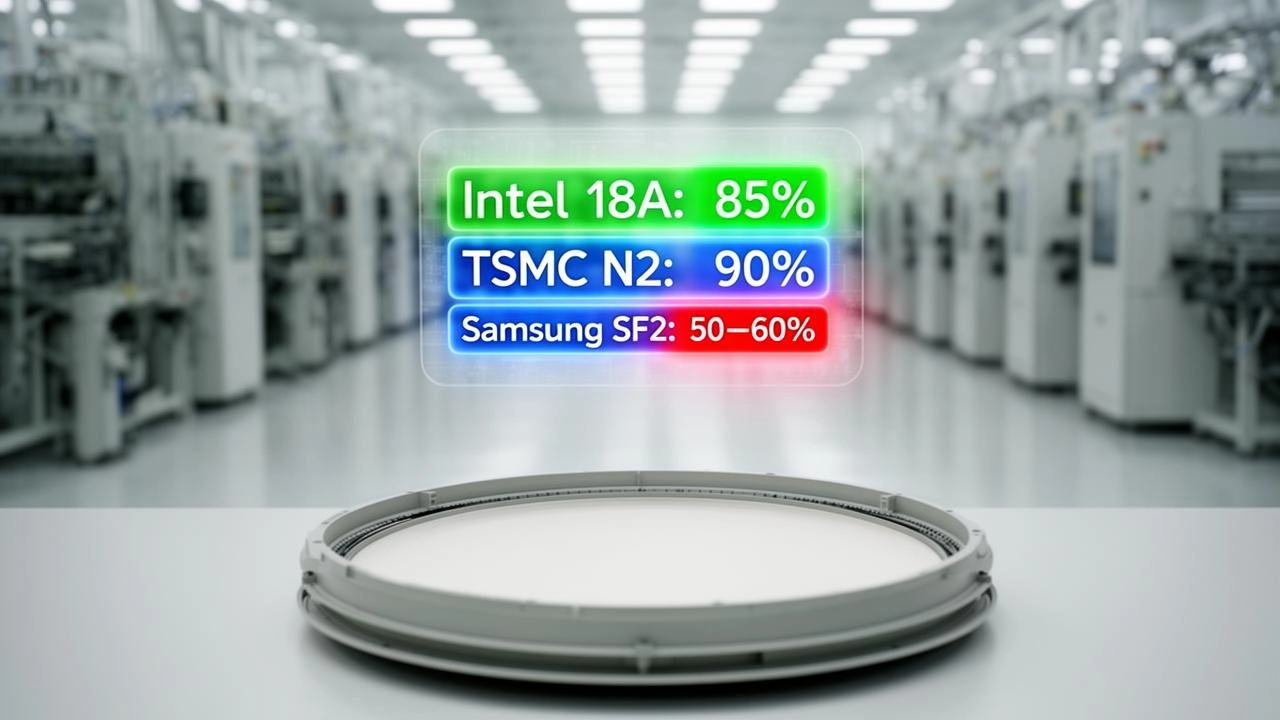
The core story is simple: Intel’s manufacturing is no longer the punchline of the PC hardware world. According to a KeyBanc Capital Markets report, Intel’s 18A process yield has jumped from 65% to 85%, closing in on TSMC’s 90% N2 yield and comfortably beating Samsung’s reported 50–60% on SF2. For a bleeding‑edge node, 85% is not a lab curiosity; it is the threshold where mass production starts to make economic sense. This is why the same report ties the yield jump to design wins from AMD, NVIDIA, Marvell, Microsoft, Micron, and OpenAI. When your fiercest rivals are willing to send you their crown‑jewel designs, it means they believe you can ship in volume, on time, at competitive cost.
Rivals as Customers: Why AMD, NVIDIA, and OpenAI Are Knocking
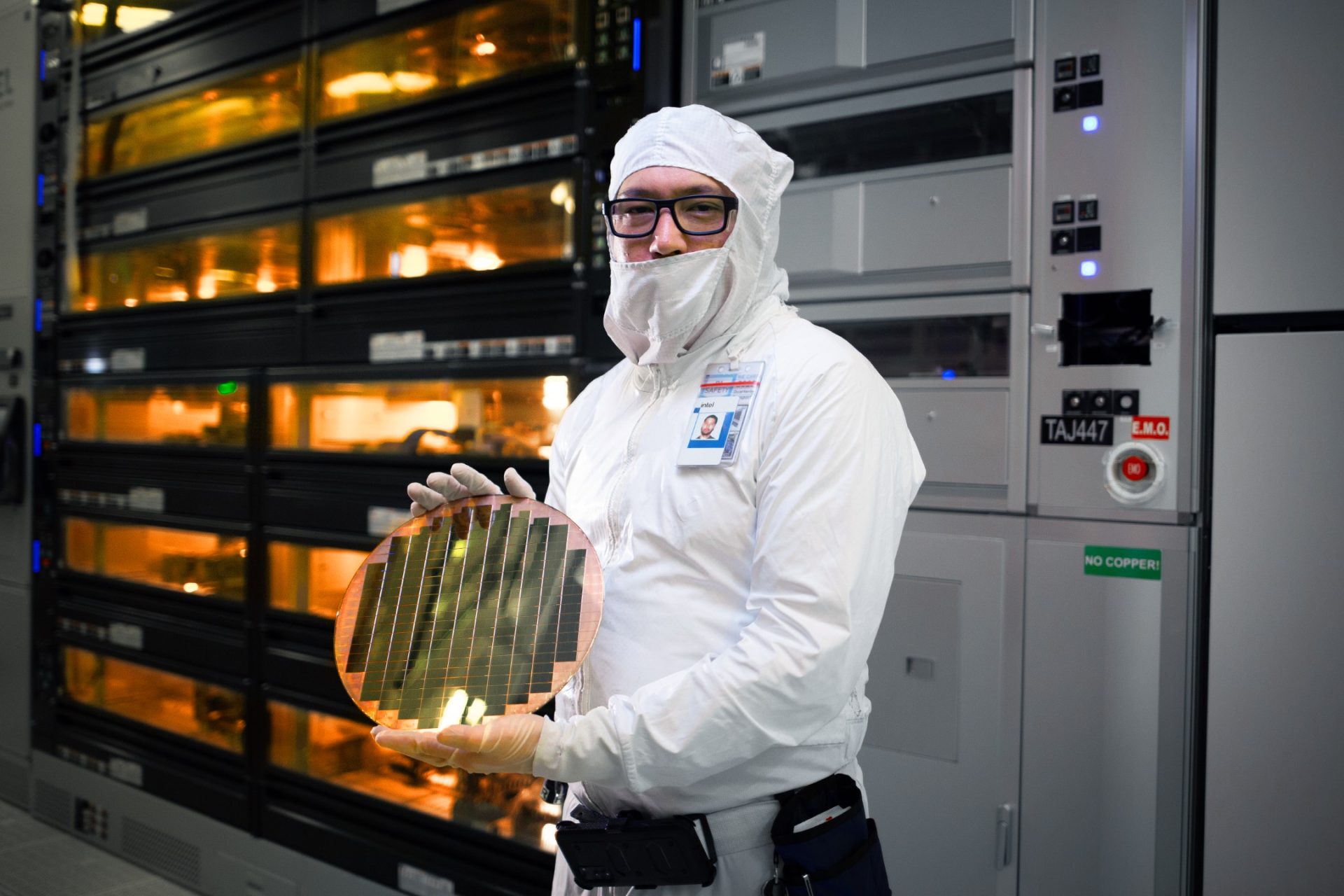
The most striking part of the Intel foundry story is not the yield chart; it is the customer list. KeyBanc and FactSet report that Intel Foundry has secured design wins with AMD, NVIDIA, Marvell, Microsoft, Micron, and OpenAI on its 18A and 14A nodes. This is the definition of competitors voting with their wallets. These companies are not sentimental; they are desperate for capacity at advanced chip manufacturing nodes that can sustain AI and GPU demand, while traditional leaders are constrained.
Intel’s own history of process delays makes this shift even more telling. For AMD and NVIDIA in particular, betting designs on Intel 18A is an explicit hedge against being limited by one dominant foundry. Heightened shortages at the leading fab have turned Intel into a suitable alternative for high‑performance silicon, especially as 18A ramps and 18A‑P moves through risk production. If these designs tape out and ship smoothly, the phrase “NVIDIA AMD Intel partnership” will stop being a headline gimmick and start being a structural feature of the GPU and AI supply chain.
Packaging Catches Up: EMIB at 98% and the System-Level Battle
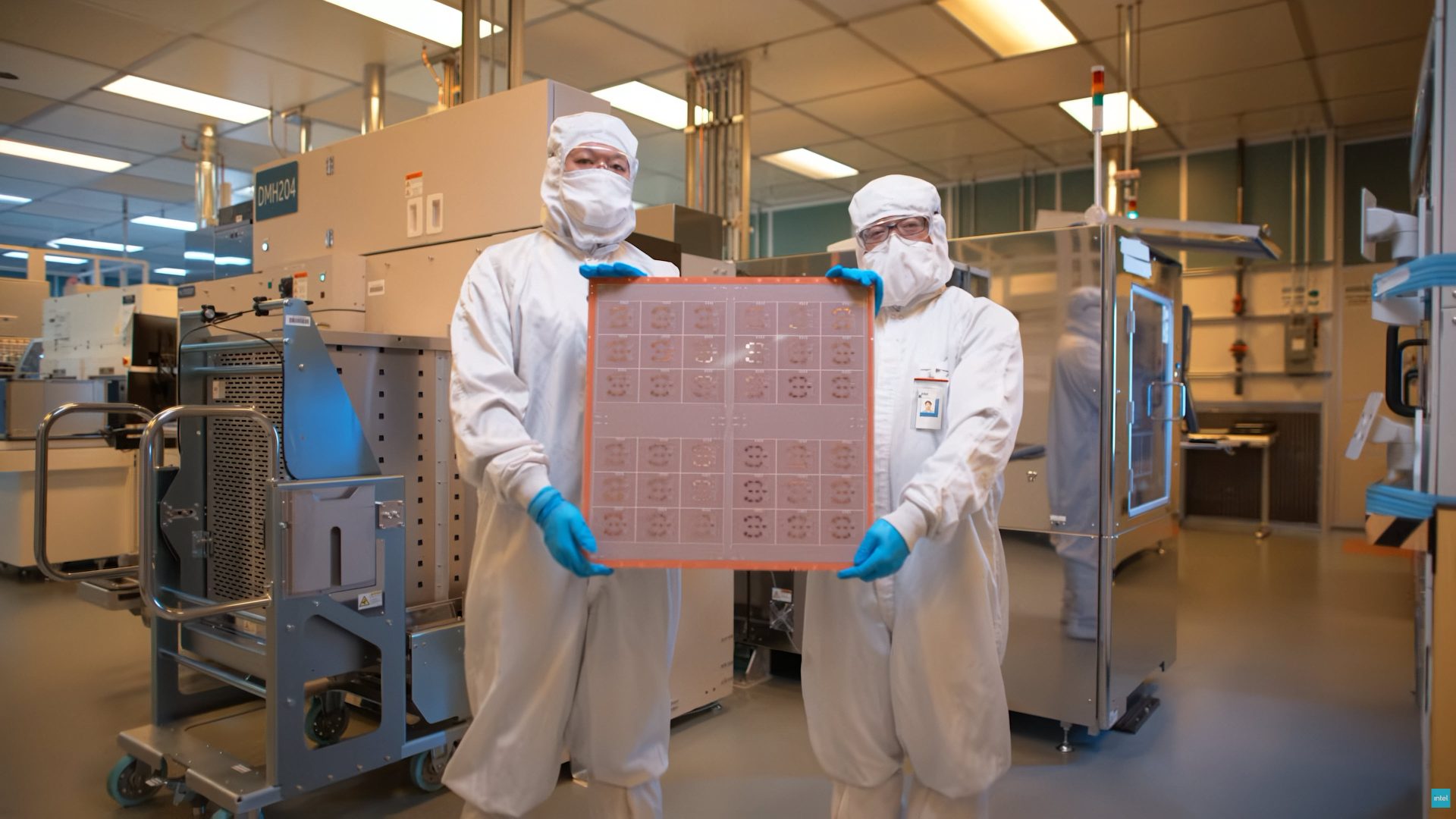
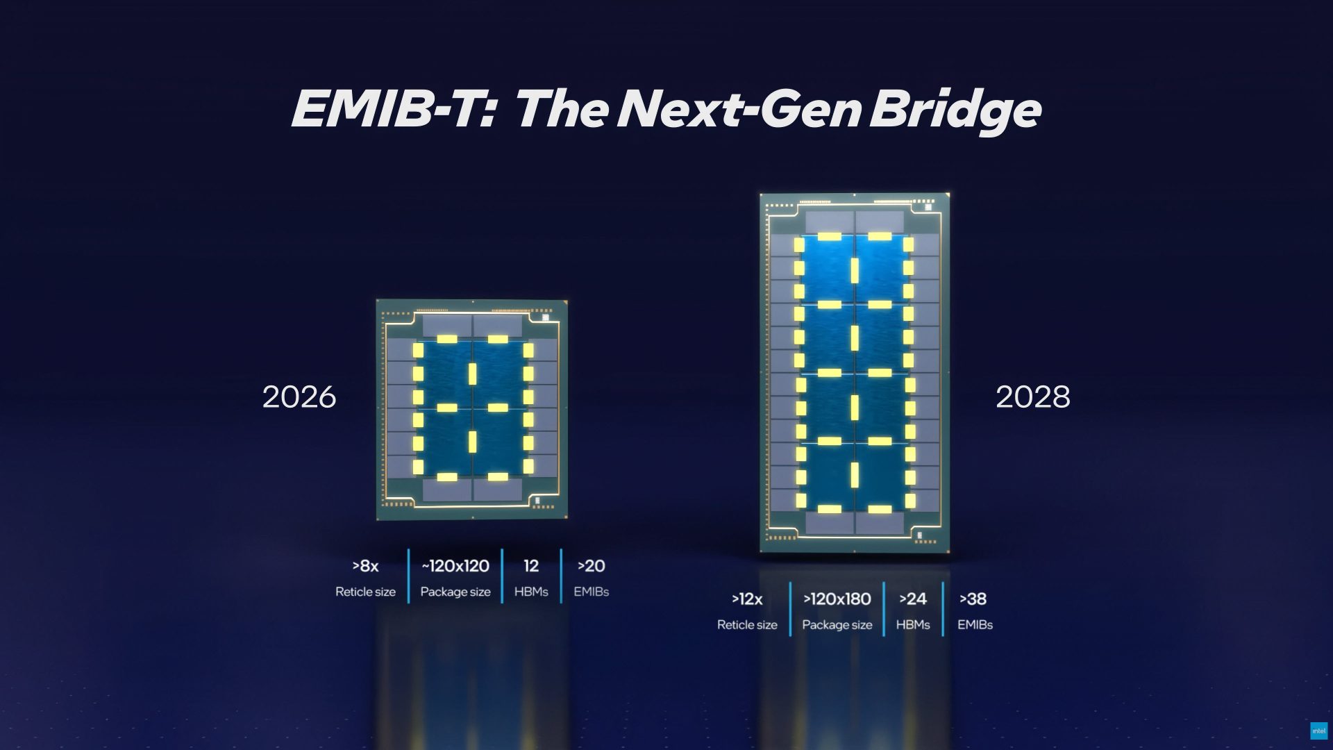
Advanced chip manufacturing in 2026 is not only about transistor size; it is about how you stitch many dies together. Here, Intel’s EMIB packaging story matters as much as 18A. The KeyBanc report says EMIB‑T yields have climbed from 90% to 98% in about three months, matching the 98–99% range reported for the leading CoWoS packaging. Hitting that last few percent is notoriously painful; reaching it means packaging is now a competitive weapon, not a liability.
This is why some of the most advanced accelerators—such as NVIDIA’s Feynman GPU, Google’s TPU HumuFish, and AWS’s Trainium 3—are already using Intel EMIB packaging. Intel is also pushing toward glass substrate packaging at its dedicated facility, aiming at larger, more complex system‑in‑package designs that traditional organic substrates struggle to handle. In other words, Intel is no longer chasing solely on process; it is contesting the whole stack: node, package, and system design freedom. That directly affects how big future GPUs and AI chips can get, and how flexibly vendors can mix CPU, GPU, and HBM tiles.
From CPU Giant to Systems Foundry: How the Business Model Shifts
Foundry success gives Intel something it has lacked for years: a second growth engine that does not depend on keeping x86 PC CPUs dominant. KeyBanc’s report links the dual breakthroughs in technology and customers to a more optimistic outlook on Intel’s valuation and long‑term earnings power. Analysts expect foundry expansion and high‑margin EMIB‑T ramp to support revenue and EPS growth through 2030. That is Wall Street language for “this is no sideshow.”
Internally, this is already changing behavior. Intel had planned to outsource 60–70% of its next‑generation Nova Lake desktop dies to a competing 2 nm process, but with 18A yields improved it now intends to keep 80–90% of those dies in‑house. The report explains this pivot by pointing to rising competitive tension and less favorable pricing and support Intel faces at external fabs. At the same time, Intel is increasing equipment orders for 18A and Intel 3 capacity by about 30–40% to meet rising AI‑driven demand. The message is clear: Intel wants to be both a top CPU designer and the neutral manufacturing backbone for many of its rivals.
What It Means for the Next Wave of PC and AI Hardware
If Intel can sustain this momentum—18A at 85% yield today, 18A‑P in risk production, and 14A slated for risk production in 2028 and volume in 2029—then the duopoly in high‑end manufacturing turns into a true race. The 14A roadmap, with defect density already tracking better than 18A, underlines that Intel is planning beyond a one‑node comeback. At the same time, the strong rise of Intel Foundry aligns with policy‑level support, which is clearly backing a more diversified manufacturing base.
For PC and AI hardware, more viable fabs means more negotiating power for chip designers and less risk that one overloaded foundry throttles the entire industry. Design wins from AMD, NVIDIA, and OpenAI signal that Intel 18A and eventually 14A are becoming viable options for the most demanding CPUs, GPUs, and accelerators. Whether Intel can turn this into a full challenge to the current manufacturing leader is still an open question, but the old assumption—that there is only one place to build the fastest chips—is already broken. That shift alone will shape what kinds of processors enthusiasts, professionals, and data‑center buyers see in the next generation.